-
• #2
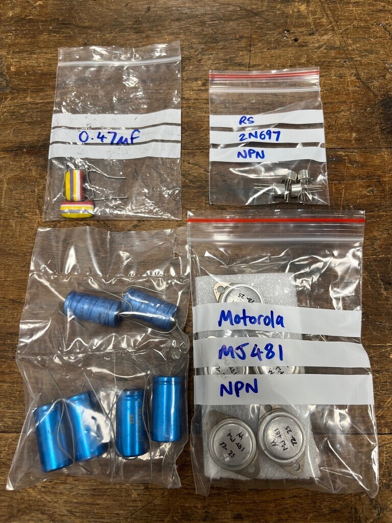
I also found some 2N697 transistors for the driver stage. I specifically wanted transistors in the older metal cans rather than the more modern plastic ones. I guess these ones might be 1980s or 1990s but they don’t look earlier than that. What I didn’t seem to be able to find were any 2N3906 PNP transistors in an old-style can. The design notes mention that the most critical transistors in the design are the 697s but that the 3906s are not that important. I’ve got loads of 3906s at work because they’re just a cheap, general purpose PNP. so I figured I could probably use a couple of those to start with and swap them if a a couple of old 3906s or 4058s turned up.

I bought a couple of the cheap eBay JLH 1969 amplifier kits, cheapest ones I could find, with the plan to dump all the components and just use the PCBs and hardware.
For the capacitors, again, I wanted to use old ones. I had most of the big ones in my stash but not 100uF and 220uF Philips ones at high enough voltage, so I went on eBay and found some. Planned to use a couple of Mullard tropical fish ones from my stash for the input coupling and apart from the 3906 transistors in metal cans, I had pretty much everything I needed to get going.
-
• #3
The power supply on a class A amp is a funny thing. It runs flat-out all the time, so it’s not subjected to sudden current demands like on a class B or later amp. That means it doesn’t suffer from the associated voltage fluctuations that happen when the current demands vary, so the output and amplification don’t vary either. What that basically means, if I’ve understood it correctly, is it’s quite suited to a regulated voltage. The original paper suggested this as a design:
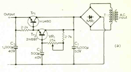
According to the notes, that should have made a circuit with variable voltage. I couldn’t get it to work even when loaded, and swapped the position of VR1 and the 2.7k resistor to make a voltage divider:
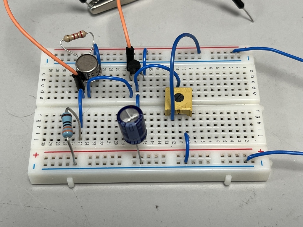
That worked just fine. I used a 3904 NPN and a 2N3035 in place of the MJ480, but the gain/outputs should be the same.
However, any ripple is replicated through the circuit, just at a higher current, which sort of defeats the object. I want the amp to maintain vintage components but I’m not all that bothered by the power supply. I just want it to hold its voltage steady at the correct voltage. I’d bought five MJ481s so I had the fifth one for the power supply, but actually a later dedicated voltage regulator would probably be better. In steps the LM350:
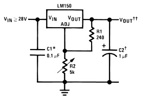
The advantage is that the LM350 makes a reference voltage internally and bases its output on that rather than as a percentage of the input voltage, so it doesn’t matter what goes in, the output voltage is always constant.
The basic circuit worked fine and I wanted to know what sort of heat it would kick out under load. So I repurposed my home made battery discharger that I’d cobbled together to test the hybrid battery in my Honda Insight because that had a 50W 15R resistor sat on a piece of aluminium extrusion.
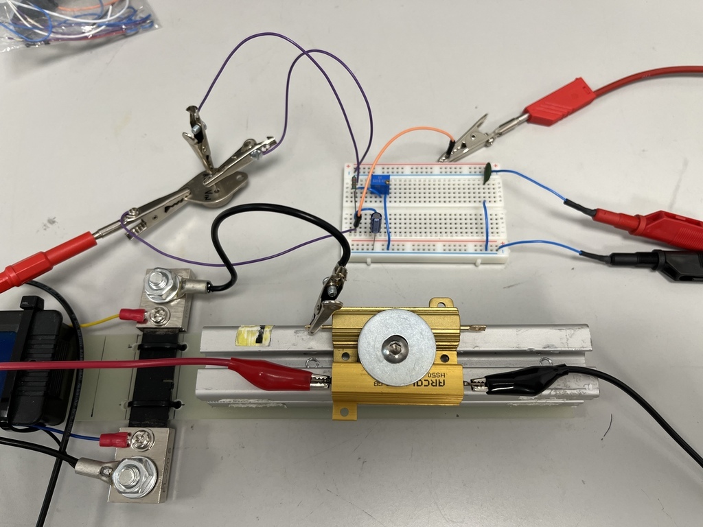
Short answer was it kicked out a lot of heat and it’s going to need a lot of heatsink to keep it cool. No worries, I have heatsinks.
The final part of the puzzle was the PNP input transistor. I said before I wanted to use old components but I couldn’t find a 3906 PNP transistor in an old metal package, only the more modern plastic ones. I narrowed it down to a 2907 which looked close enough, but I wasn’t 100% confident. I spotted that the modern JLH circuit diagrams actually have a modern 2907 specified, so that gave me a bit more confidence that I was interpreting the data sheets correctly.
-
• #4
Onto the start of the build. Reusing the PSU case for the amp case, this was a potential layout. Heatsinks for the power transistors are on the back. The one in the middle is for the PSU. Not the best layout in the world due to the shape of the case, but I was thinking a big grounded heatsink for the PSU would provide a bit of shielding for the amps from the huge transformer.
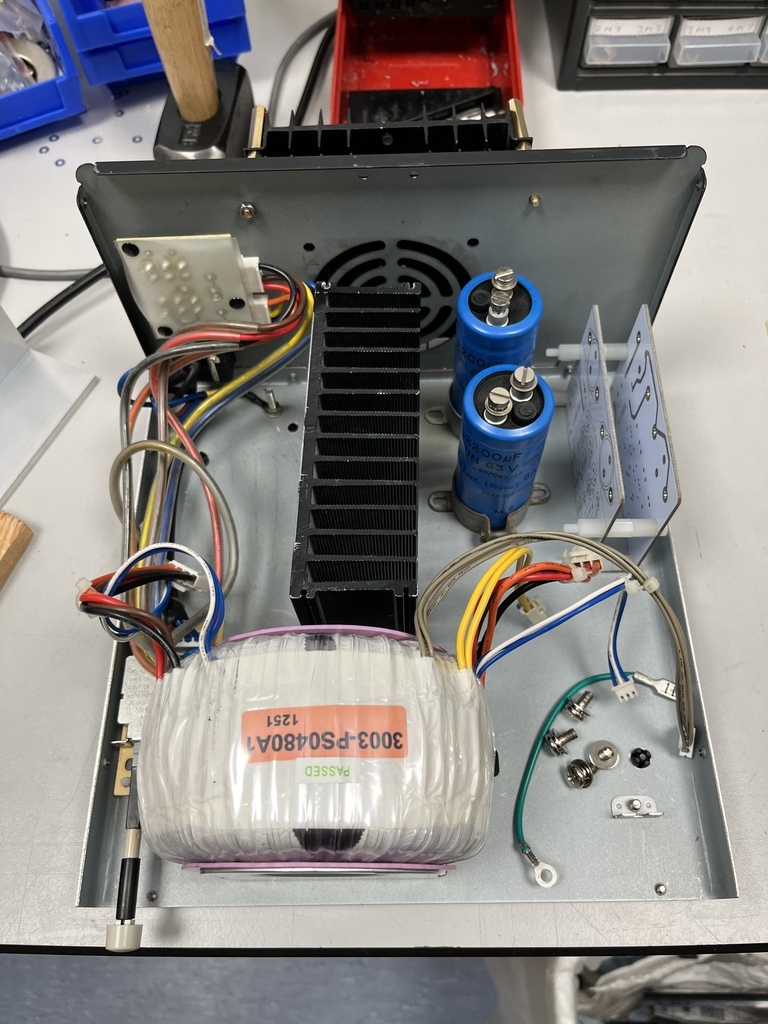
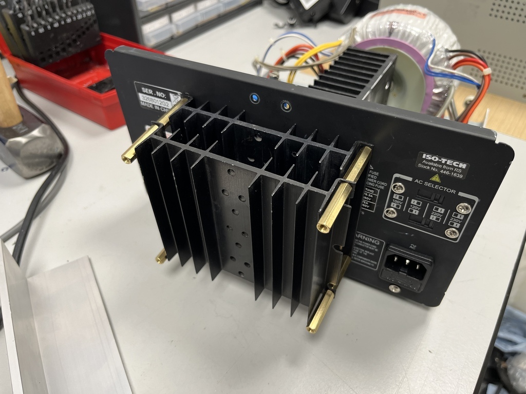
One annoying thing with this case is the front panel is kind of fundamentally part of the structure. I figured if I could slice the frame off it somehow, I could bond a fresh front panel onto it.
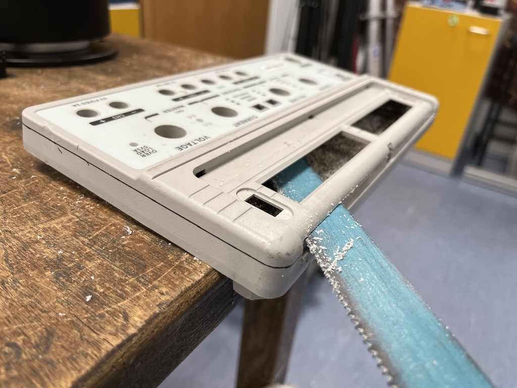
This seemed like a good idea at the time. Over an hour later, and sore arms and hands, I had this:
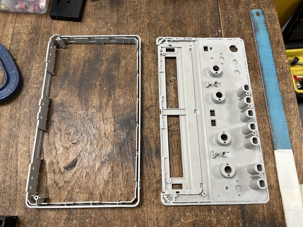
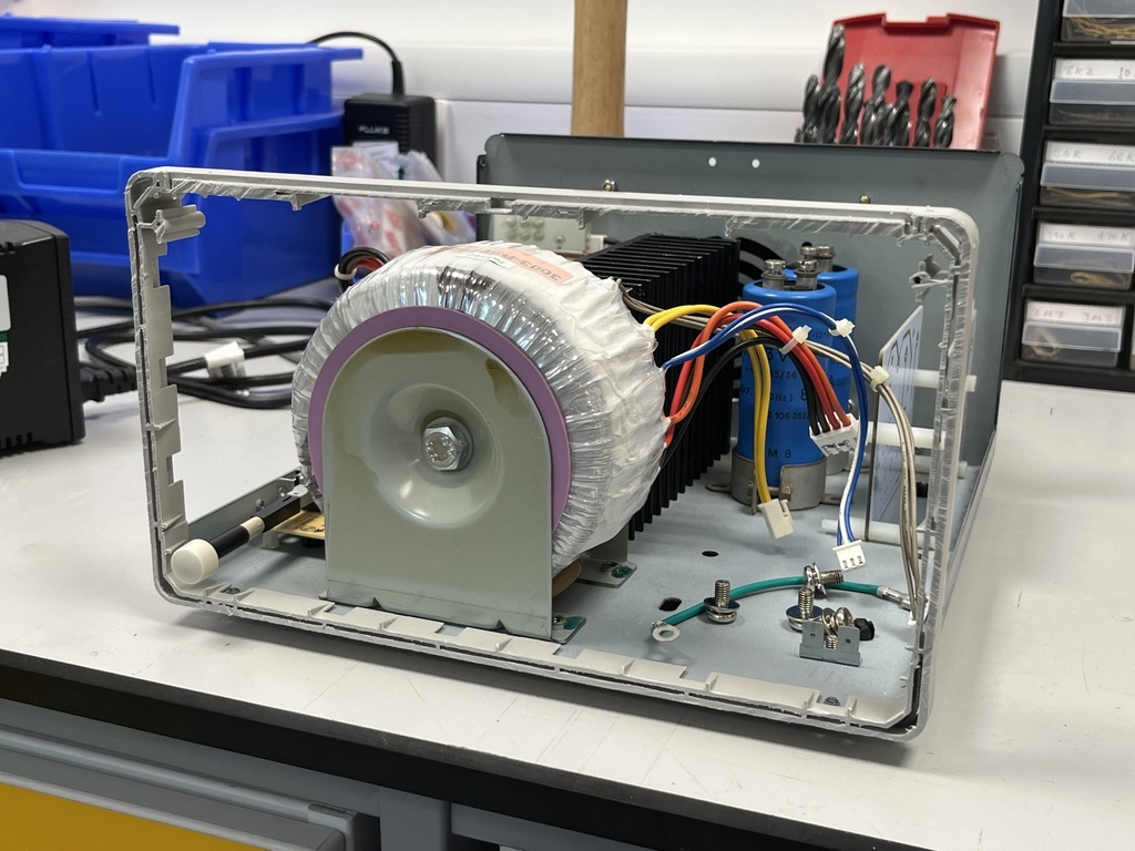
-
• #5
I’ll concede that I understand at best ~20% of the above word but I am nevertheless hooked…
-
• #6
Love it. Subscribed.
-
• #7
I made a start on the PSU:
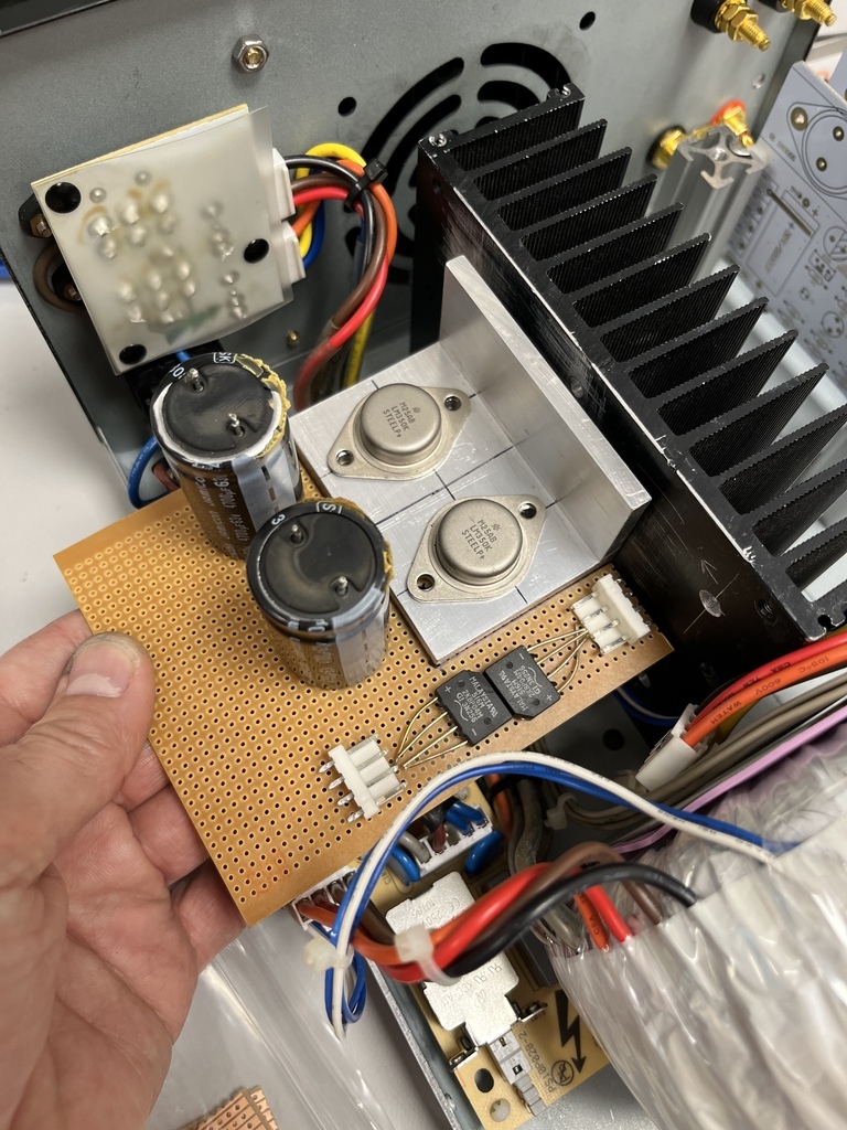
Some thick angle which was an offcut from a work project. When I loaded up the LM350 with 2A, it got extremely hot. Loaded with 1A though it kicked out hardly any heat at all, so I decided to double them up. I put two in parallel, but they actually ended up fighting each other and one of them ended up doing all the work. So I thought a better idea would be to use both the 3A secondaries on the transformer, rectify both separately and run separate regulated supplies to each channel. I should be able to match the voltages to within 0.1V or better and it’ll save driving anything flat out or resorting to balancing resistors or using op amp voltage tracking. I’m aiming for strictly analogue and through-hole, no ICs!
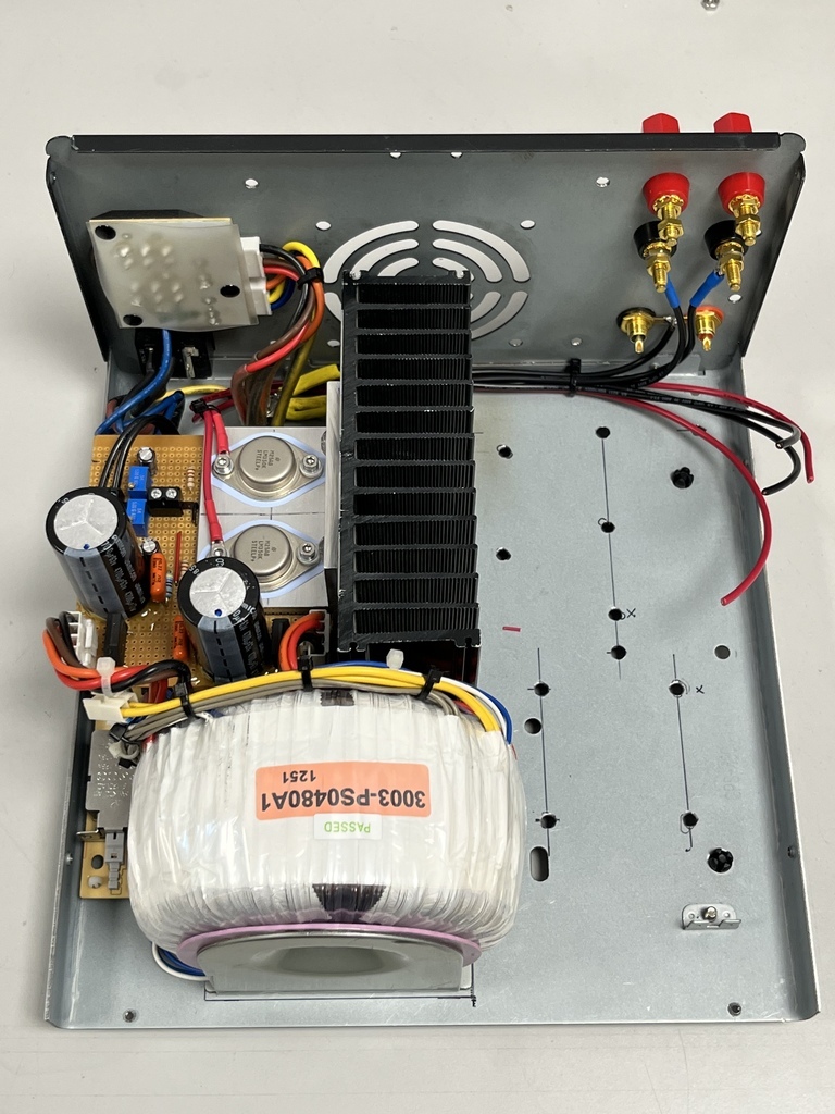
That then brings us up to date. This is the 2x 27V 3A power supply built. Tracks reinforced with thick solder runs to handle the current. It actually goes up to about 55V and I could run it up at about 40V for a bit more output, but I’ve got it wound right down as per the OEM design. Got each channel within about 0.05V of each other which should be good enough:
I’ve mounted up the output transistors and added some wires to wire them in:
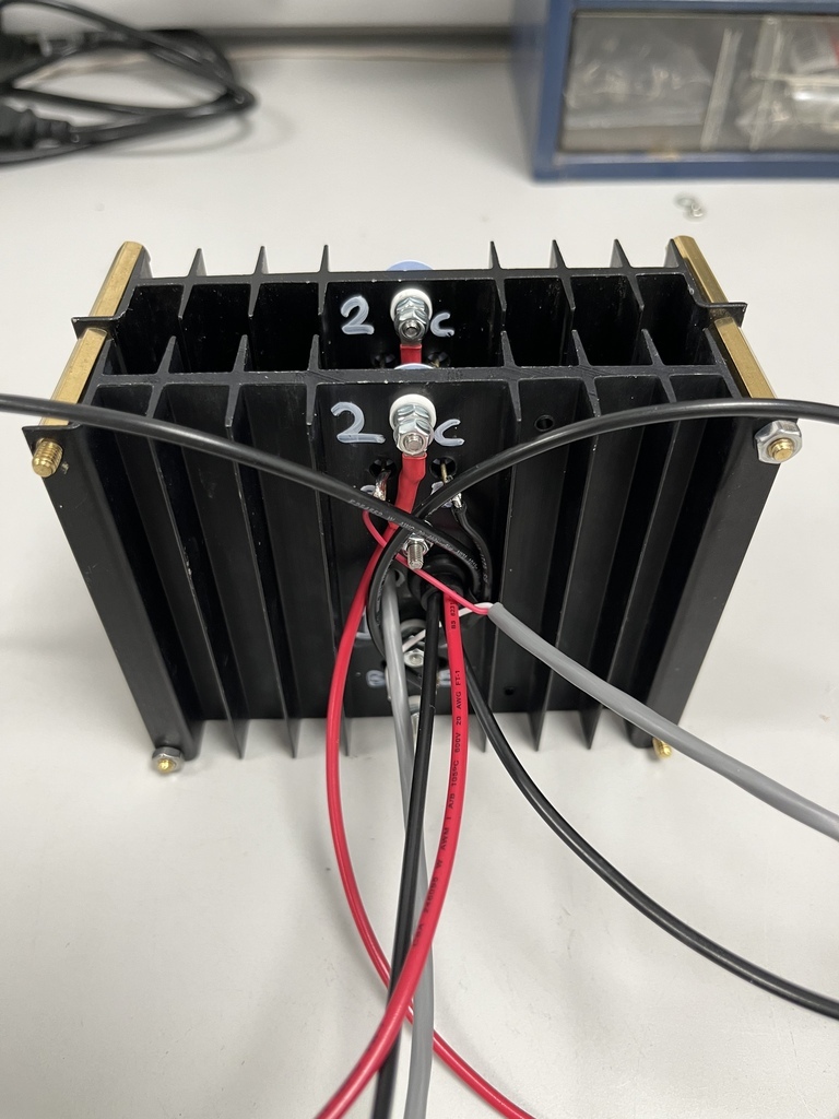
Note I used a paint pen to mark B, C & E on the heatsinks to make sure I got the wires in the right place. That’s this part of the circuit and the rest will be on the PCBs:
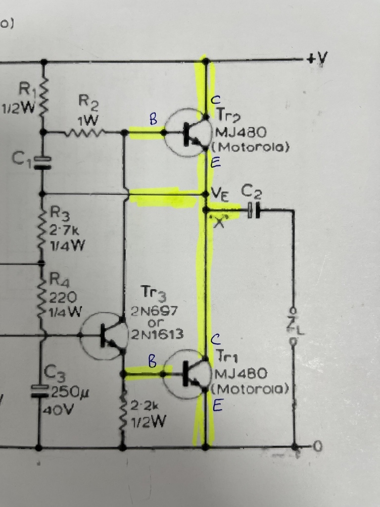
I’m not 100% happy with that, specifically the layout, because it’s a mess of wires carrying signals and power, all crossing over each other and poking through holes and it won’t surprise me if it picks up some noise. I’ll just have to wait and see what it does and if it’s a problem I’ll reconfigure it.
The side you can see looks much better:
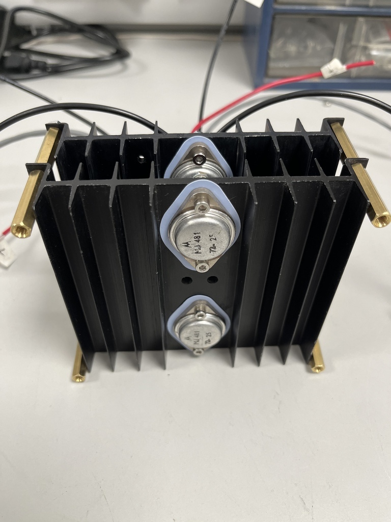
There will be a cover over that because the transistor cases are live.
-
• #8
I’ll concede that I understand at best ~20% of the above word but I am nevertheless hooked…
Haha, I’ll try and keep as much of it in plain English as possible 😀
-
• #9
It was published in 1969, hence the name, and has been difficult to surpass in terms of simplicity
And that was the last bit I understood
-
• #10
Like most I have no idea what's going on aside from my A level physics but admire your ingenuity
Taking stuff from waste at work is not allowed where I work.
-
• #11
Same as others, I can read the words but this is soooo far beyond my very limited sphere of knowledge. But I'm appreciating the skills, reclamation, research and more going in to this! Looks like a great project. I think.
-
• #12
I guess these ones might be 1980s or 1990s but they don’t look earlier than that.
Week 5 1981 is my guess
Fun project
-
• #13
Week 5 1981 is my guess
That’s probably correct. That picture is from the eBay ad, I don’t think I actually checked what was on the ones that turned up in the post!
-
• #14
Subbed
-
• #15
I'm so here for this.
-
• #16
I partially soldered up the amplifier boards at lunchtime. Missing a couple of resistors so I couldn’t quite finish them. See how I’ve moved some of the capacitors and bulky components around so they’re between the boards - purely for packaging reasons because it’s a tight squeeze.
I’ve decided I hate 2-sided PCBs with plated through-hole connections, especially when the holes around the component legs are so tight. Presumably for cheapness reasons. They’re a right pain to solder.
2 Attachments
-
• #17
Slight diversion. Key bit of information I left out was that the JLH build will almost certainly end up in the living room. I still needed a small amp for the spare room so I did indeed indulge in a cheap eBay kit. They’re all much of a muchness, based on Chinese clones of long-obsolete ICs and there are loads to choose from. I settled on a stereo pair of TDA2030s, mainly because it was one of the kits that came on a single board and I didn’t want the hassle of mounting two boards and having to buy extra stuff like a dual pot of the volume control. But also because it was class AB, through-hole, it had convincing-looking heatsinks designed in and it had bass and treble onboard. This quick build was pretty much all parts bin stuff or recovered/scavenged parts. £5.53 delivered for the amp, a couple of £ for the RCA jacks and speaker posts and I’m pretty sure the rest was all stuff I’d pulled out the bin.
As usual, my old nemesis the hum was in full swing. First thing I tried was more PSU smoothing, by bodging in a couple of extra smoothing capacitors, but it became obvious that it was where I’d remote mounted the pots for volume, bass and treble. The wires I used were unshielded and were picking up noise when I moved my hand near them. I thought about doing something properly but in the end just rolled them in aluminium foil from the kitchen and earthed them. It’s not completely got rid of it but most of it is gone.
That all happened because I wanted some ventilation out the back so put the potentiometers on wires instead of directly on the board. Hindsight. Probably should have split out the TDA2030 ICs on their heatsinks instead.
Anyway, it’s class AB so it sounds ok. Probably kicks out about 5-6W per channel but that’s all I need. Stuck some knobs on from the PSU case from the JLH build and that’s all it needs.
3 Attachments
-
• #18
I got the transistors and power supply wired in to the right hand channel after work. Took a lot of figuring out and cross-comparing to the circuit diagram to check I got the connections in the right place. I
wasn’t brave enoughran out of time to fire it up, I’ll see if I get time later in the week.
1 Attachment
-
• #19
I completed the electronics part of the build. First power-up is always nervous as, although you check everything, you never really know if you've mis-wired something and you sort of flick the switch and hope nothing goes bang. Well, nothing did, which was good news!
There are two things to set up on these: the voltage midpoint at the output transistors and the quiescent current.
The voltage midpoint needs to be set because this original design used a single rail power supply (0-27V) and a big output capacitor to block the DC getting to the speakers. On a modern amplifier you'd use +/-15V and eliminate the capacitor because the midpoint sits at 0V. On this design it needs to sit halfway up the supply voltage so that the signal can swing between 0V and and +27V at point VE or 'X' on the circuit diagram below. That voltage point is set by resistors R5 and R6. If all components were to exact spec, that should be the case, according to the original notes. The kits don't bother with this and use low tolerance resistors and trim pots so you can make adjustments. I didn't want to do it that way, so I used 1% tolerance resistors throughout and selected ones with values which were the closest to book value.
However, my VE value on the right-hand channel was still out by a volt. The reason for that is probably tolerances on the transistors. This would affect the output and the quiescent current, so I swapped out R6 for a 27k resistor and 100k trim pot in series, as per the kit version. I could then adjust the voltage back up from my measured 12.69V to the ideal 13.59V (my supply is 27.18V).
Onto the quiescent current. I disconnected the power supply rail and ran it through my multimeter on the 10A scale so I could read the current being drawn. 1.21A and the ideal when running an 8 Ohm speaker is 1.2A, so I was happy with that.
I repeated all the above with the left-hand channel. The only thing I found was the quiescent current was measuring 1.37A on that side. On the kits, again, they have a trim pot to set the quiescent current instead of using a close tolerance resistor. The main issue with trim pots in this part of the circuit, is they are actually under spec for the current going through them. So I've opted to stick with the resistors. If I've understood this correctly, if the quiescent current is too low, it will starve the output stage at high outputs. If it is too high, it is simply wasting power and it gets dumped out as heat onto the heatsinks. So I've opted to leave it, since it's only 170mA.
2 Attachments
-
• #20
Once it was all tested up I could fully install the modules and add a volume pot. I've always found these fiddly to solder directly to the pins, so I opted to stick a bit of Veroboard on the bottom and solder the wires to that. Did it make it easier? No. But now I know! I still labelled it carefully so as not to make any mistakes and also soldered on some ground wires to the pot case.
When I get a chance I'll sort out a front panel and tidy up the case.
2 Attachments
-
• #21
So, onto testing at home. This is my first time with a class A transistor amp. All my previous transistor amp builds have been class AB, which sort-of run in class A at low outputs and switch to class B as the output increases above the quiescent value. I made some notes while messaging a friend who's also into electronics.
First thing is it definitely needs more cooling. I thought the heatsinks I used would be adequate but longer-term it's not going to do the transistors much good running that hot.
It has big, deep bottom end. The transient response is sudden, like unexpectedly so, and can take you by surprise for something that’s only putting out a couple of watts. I think it’s because the power supply doesn’t drop any volts when the music suddenly gets louder. This is a thing that class A amps shine at - on a class AB or B amplifier, even a big one with a big power supply, the power supply voltage drops as you make bigger demands on it. This means the amplification drops as well, so you don't get completely linear amplification between zero output and full output. On a class A amplifier you do. This one draws a constant 1.2A on each channel no matter what it’s doing, plus I’ve regulated the voltage so it just sits bang on 27V and doesn’t move.
So some tracks like Tasmin Archer - Sleeping Satellite and Moody Blues - Nights in White Satin have a lot more depth than usual. It’s less noticeable with electronic music which doesn’t have so much dynamic range. But for example I had Death in Vegas - Dirge playing and, although I was used to it building, it just got louder and louder and louder as the track went on. Sash! - Encore Une Fois sounded massive and I only had it turned up to a couple of watts.
Another thing is bass guitar sounds very detailed and you can hear the string detail on it as well as the bassline. My pal speculated this is the lows not swamping the higher frequency stuff, where class AB probably sags the supply voltage and takes out the details. As the supply voltage on this does not change, it does not do that.
My main amp at home is a pair of 150W Maplin MOSFET amps, another home-build that I originally built in the mid-90s and rebuilt in 2021. That's an AB design and it's always sounded great on my big speakers. I’m very tempted to make a regulated supply for the that amp. I bet it would have some attack!
-
• #22
Love this, it reminds me of hanging out with my dad. He’s just an electronics nerd not an electronics + audio nerd, but i still get the same enjoyable feeling of being miles out of my depth.
-
• #23
Glorious, thanks for this thread.
Put some Prince through it please. -
• #24
Haha, great stuff!
-
• #25
Glorious, thanks for this thread.
Put some Prince through it please.That is a good shout.
 Jonny69
 drøn
drøn branwen
 midlife
 si_mon628
 Five-Hats
 Sparky


 Arvy.
Arvy.
I started this a short while back. I’m currently partway through the build of a John Linsley-Hood ‘1969’ amplifier. This is a seminal amplifier design that defined all future class A designs. It was published in 1969, hence the name, and has been difficult to surpass in terms of simplicity and sound quality.
First a bit of background. I have some previous with vintage amplifier design and build, and I’ve built a number of valve amps and other bits of kit going back to when I was a teenager. I work in a lab which has a fair turnover of old electronic kit and regularly manage to pull things like scopes and power supplies out the WEEE bins. Some works, some doesn’t, but this stuff tends to donate a lot of parts to my builds.
So, I needed a small amp for upstairs and I was going to build something. Easiest way would be to use one of my many power supplies and a stereo class D module from eBay. This one would be ideal:
Fix it at the 15V setting and use the hole for the volume pot. Add inputs and outputs, job done.
But how about a new rabbit hole instead, because that would be far too easy. I’m thinking what about something iconic like the John Linsley-Hood 1969 class A transistor amp, using new PCBs but built with vintage transistors and the Philips capacitors from my stash.
Why complicate it and add loads more expense? Well, I kept getting videos about the cheap Chinese JLH amp clones with fake 3055 transistors popping up on my YouTube feed. They are available pretty cheap as kits with all the components, PCBs, heatsinks and the hardware for mounting those T03 transistors. I can't buy a pair of PCBs, heatsinks and hardware individually for the price the kits, so I figured I could just bin off the cheap components and swap in better quality ones, and basically replicate the original sound by using old transistors and capacitors.
Resources:
Wikipedia article on John Linsley Hood: https://en.m.wikipedia.org/wiki/John_Linsley_Hood
It says in there that it was published in Wireless World in 1969 (April 1969 issue, p. 148).
ORLY? So it is: http://www.worldradiohistory.com/hd2/IDX-UK/Technology/Technology-All-Eras/Archive-Wireless-World-IDX/60s/Wireless-World-1969-04-IDX-75.pdf
So to stop this getting ridiculously expensive, I needed a power supply. A couple of months ago I pulled a 2x 30V @3a digital bench supply out the WEEE bin. Only one channel was working so I popped it open to see if I could fix it. It was a bit frazzled on the dead channel so I pulled off a couple of heatsinks for a pal and tossed it back in the bin. Amazingly, when I looked a couple of weeks later it was still in there so I pulled it back out to recover the transformer. Here it is:
When I said it had got a bit frazzled, I mean it had cooked itself. Properly. You can see it got a bit hot just from the circuit board:
But with the heatsink pulled off I reckon it must have been smoking a bit when it popped the fuse!
This all happened because the fan had packed up and jammed. And the thermal cutout clearly worked well on that model.
Anyway, with the rectifier board etc pulled out the case, this was what I was left with:
The transformer itself worked fine. The two secondaries put out 33.7V AC which is ideal for this project.
I started this at the end of Jan but I’ve got a decent chunk of the build to post up to get us up to date. The thing that kicked this off for sure was I found some unused original spec output transistors on eBay. Motorola MJ481, as specified in the original JLH 1969 design, and dated 1972. So that meant a full vintage build was possible.